Light Speed Ahead: The Future of Computing with Co-Packaged Optics
Electrical interconnects are struggling to keep up with the demands of AI and high-performance computing, paving the way for revolutionary optical solutions.
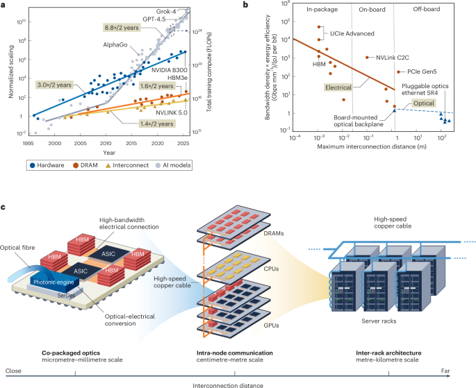
The escalating data demands of artificial intelligence and high-performance computing are pushing traditional electrical interconnects to their absolute limits, necessitating a transformative shift to co-packaged optical technologies.
The Looming Bottleneck in Modern Computing
The landscape of modern computing, particularly in the realms of high-performance computing (HPC) and artificial intelligence (AI), is characterized by an insatiable hunger for data movement. As computational capabilities advance exponentially, the ability to efficiently transfer vast quantities of data between processing units becomes the critical choke point. Traditional electrical interconnects, which have long served as the backbone of digital communication within chips and between components, are now encountering fundamental physical limitations. These limitations manifest primarily as resistive losses, where electrical signals lose energy as heat, capacitive loading, which slows down signal transmission, and frequency-dependent distortion, compromising signal integrity at higher speeds. Together, these issues severely constrain bandwidth, increase latency, and diminish energy efficiency, threatening to impede the continued progress of cutting-edge computing applications.
The implications of these electrical bottlenecks are profound. For AI workloads, which often involve massive neural networks requiring constant data exchange, inefficient interconnects translate directly into slower training times and higher operational costs. Similarly, HPC tasks, ranging from complex scientific simulations to financial modeling, rely on seamless, high-speed communication between thousands of processors. When electrical connections falter, the overall performance of these sophisticated systems suffers dramatically. The industry recognizes that without a fundamental paradigm shift in how data is moved, the envisioned future of hyper-converged, data-intensive computing will remain out of reach. This pressing challenge has led researchers and engineers to explore alternative communication methods, with light, or photonics, emerging as the most promising successor to electrons.
Embracing Light: The Promise of Optical Interconnects
The solution being aggressively pursued is the development of optical compute interconnects (OCIs). This innovative approach involves replacing the problematic electrical links with co-packaged photonic channels, effectively transmitting data using light pulses instead of electrical currents. The advantages of optical communication over electrical are significant and directly address the shortcomings of current systems. Light, by its nature, experiences minimal propagation loss, meaning signals can travel further with less energy degradation. This translates into substantially higher bandwidth capabilities, allowing for an immense volume of data to be transmitted simultaneously. Furthermore, optical signals exhibit superior signal integrity, being less susceptible to electromagnetic interference and distortion, ensuring data arrives accurately and reliably. The result is a system with reduced latency, improved energy efficiency, and a far greater capacity for data throughput.
Integrating these photonic channels directly with electronic chips, a concept known as co-packaged optics (CPO), is the key to realizing these benefits. Instead of routing electrical signals across circuit boards and through numerous discrete components, the electro-optical conversion happens very close to the processing units. This minimizes the length of problematic electrical traces, pushing the performance barrier from the physical limitations of copper wires to the almost limitless speed of light. The transition to optical interconnects is not merely an incremental upgrade; it represents a foundational change in how computing architectures are designed, promising to unlock new levels of performance and efficiency essential for the next generation of AI and HPC systems.
Architectural Innovations for Integration
The journey towards widespread adoption of optical compute interconnects involves a sophisticated interplay of various technological domains. To achieve optimal system-level performance across critical metrics like bandwidth, energy consumption, and latency, researchers are meticulously analyzing and optimizing three main areas. First, the electrical subsystems that interact with the optical components must be efficient and capable of handling the initial and final stages of data processing. This includes the drivers for optical transmitters and the amplifiers for optical receivers, which bridge the gap between the digital and optical domains.
Second, the electro-optical and opto-electronic conversion interfaces are crucial. This is where electrical signals are transformed into light pulses (electro-optical) and vice versa (opto-electronic). The efficiency and speed of these converters, often involving tiny lasers or modulators and photodetectors, are paramount. Any inefficiencies here can negate the benefits of optical transmission. Finally, the optical transmission networks themselves must be robust and high-performing. This encompasses the waveguides, optical fibers, and multiplexing technologies that guide and combine light signals within and between chips. Optimizing these components in concert is essential to delivering on the promise of OCIs.
The roadmap for CPO architectures is evolving rapidly, moving through several integration paradigms. Initial deployments might involve two-dimensional (2D) co-packaged optics, where optical and electrical components are placed side-by-side on a common substrate. A more advanced stage involves 2.5D interposer-based integration, where a silicon interposer acts as a bridge, allowing electrical chips and optical engines to be placed closer together with high-density connections. The ultimate goal is three-dimensional (3D) heterogeneous stacking, where electrical and optical layers are stacked vertically, creating extremely compact and high-bandwidth interconnects with minimal signal travel distance. Each step on this roadmap presents unique manufacturing and design challenges that must be overcome to fully realize the potential of optical computing.
Overcoming the Hurdles: Thermal Management, Manufacturing, and Standardization
While the promise of co-packaged optics is immense, several critical challenges must be addressed to ensure their successful integration as a foundational communication technology for high-performance computing infrastructure. One of the most significant hurdles is thermal management. Generating, modulating, and detecting light, even with highly efficient components, produces heat. When these optical components are integrated in close proximity to power-hungry electrical processors, the combined heat density can become extreme. Effectively dissipating this heat without compromising performance or reliability is a complex engineering problem requiring novel cooling solutions and materials.
Manufacturability also poses a substantial challenge. Integrating diverse materials and processes, such as silicon photonics, III-V semiconductors for light sources, and traditional CMOS electronics, into a single, high-volume production flow is inherently difficult. Achieving high yields, consistent performance, and cost-effectiveness at scale demands advanced fabrication techniques and innovative packaging solutions. The precision required to align optical components and ensure efficient light coupling is far greater than for electrical connections, adding to the complexity of manufacturing.
Finally, standardization is crucial for broad industry adoption. Without common interfaces, protocols, and packaging standards, the ecosystem for co-packaged optics risks fragmentation, hindering interoperability and driving up development costs. Industry collaboration is essential to define these standards, ensuring that components from different vendors can work together seamlessly and fostering a competitive market that drives innovation and cost reduction. Addressing these challenges collectively will pave the way for optical interconnects to become the ubiquitous communication backbone of future computing systems, as detailed in an article in Nature.
The Path Forward: A Vision for Scalable Performance
The ongoing research and development in co-packaged optics are not just about incremental improvements; they are about laying the groundwork for a new era of computing. The ability to move data at light speed with minimal energy loss will fundamentally alter how we design and build supercomputers, data centers, and AI accelerators. Imagine AI models that train in fractions of the current time, scientific simulations that yield insights faster, and data centers that operate with significantly lower power consumption. These are the tangible benefits that OCIs promise to deliver.
Continued advancements in materials science, chip design, and packaging technologies will be vital. Researchers are exploring novel waveguide materials, more efficient light sources that can be monolithically integrated with silicon, and advanced modulation schemes to push the boundaries of data density. The shift towards 3D heterogeneous stacking, for instance, offers a path to ultra-compact, high-bandwidth communication directly between processing units and memory, further collapsing the distances data must travel. This integrated approach, blending the strengths of electronics for computation and photonics for communication, represents a powerful synergy that will redefine the performance envelope of future computing infrastructures. The trajectory is clear: light is poised to become the primary medium for data transfer in the most demanding computational environments.
Why it matters
This fundamental shift from electrical to co-packaged optical interconnects directly impacts critical infrastructure across various sectors. For data centers and telco operations, it means drastically improved energy efficiency, lower operating temperatures, and higher data throughput, enabling the rapid scaling required for cloud computing, 5G, and beyond. Field technicians will see new maintenance protocols emerge as hybrid electronic-photonic systems become standard, requiring specialized diagnostic tools and training. For AI and infrastructure, the ability to build faster, more energy-efficient processors with reduced latency is essential for advancing complex models and real-time decision-making, ultimately supporting the next generation of AI services and networked applications.
More from Trends
RSS
Access Denied: Unable to Generate Article Without Source Content
The provided source content leads to a paywall, preventing access to the original article text. Therefore, an original journalistic piece cannot be generated.

AI's Expanding Frontier: From Cosmic Models to Corporate Strategies
This briefing explores the latest in AI, from groundbreaking universal models to its transformative impact on global employment, finance, and geopolitics, reshaping industries.

The Rise of Ollobot: Redefining Human Connection Through AI Companionship
Ollobot, a pioneering AI companion robot, is transforming how individuals experience social interaction and support in their homes, addressing a growing need for connection.