Atomic-Scale Magnetism Breakthrough Clears Path for Low-Power AI Silicon
Brown University engineers have eliminated the dead layer in ultrathin multiferroics, unlocking altermagnetism and paving the way for ultra-efficient AI hardware.
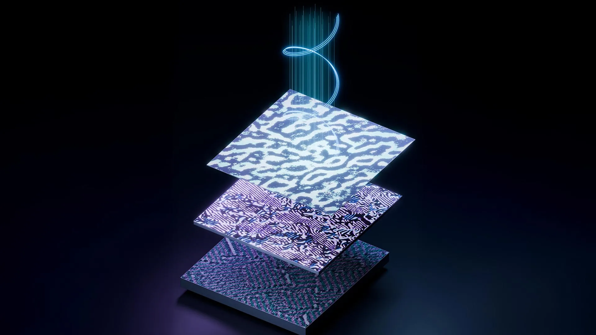
Researchers have resolved a long-standing atomic breakdown in multiferroic thin films, unlocking an exotic magnetic state that could slash energy consumption in next-generation AI processors.
Artificial intelligence is colliding with a hard thermodynamic ceiling. As deep neural networks scale in size and inference workloads expand across global networks, the electricity required to power modern data centres has ballooned. Conventional silicon microelectronics rely on shuttling electrical charge across semiconductor junctions to represent binary data. This physical mechanism inherently dissipates energy as waste heat, creating thermal throttling limits and massive cooling overheads.
For years, materials scientists have viewed multiferroic compounds as a potential escape hatch from this efficiency trap. These crystalline materials possess coupled electrical and magnetic orders, allowing a device to write data with tiny electrical voltages and read it out magnetically. Yet, whenever engineers tried to shave these materials down to the nanometre dimensions demanded by high-density chips, the properties vanished. A team of engineers at Brown University has demonstrated a technique that preserves these crucial behaviours down to atomic thicknesses, while unexpectedly generating a rare and potent magnetic state known as altermagnetism.
The Multiferroic Promise and the Dead Layer Trap
In standard computing architecture, moving electrons between logic units and memory banks consumes the bulk of a chip's total power budget. Multiferroics offer a radical alternative. In these materials, the crystal lattice contains internal electric dipoles. Applying a minute voltage shifts positive and negative ions relative to one another, reversing the material's electrical polarization with almost zero current flow. Because the electrical and magnetic orientations are physically coupled, switching the electric dipole simultaneously flips the material's magnetic orientation.
This coupling creates the foundation for non-volatile magnetoelectric memory and logic that operates at fractions of the energy required by conventional static RAM or flash memory. Bismuth ferrite, an oxide composed of bismuth, iron, and oxygen, has long been the primary candidate for such systems because its coupled states can exist stably at room temperature.
The roadblock to practical deployment has been scaling. Modern lithography packs billions of transistors onto a die, requiring functional layers that measure only a handful of atoms across. When bismuth ferrite is milled or grown into films thinner than roughly ten nanometres, it suffers from what physicists call the dead layer effect.
Two distinct phenomena cause this degradation. First, at ultra-thin dimensions, the surface atoms lose the surrounding crystal lattice that normally enforces their geometric arrangement, warping the unit cell. Second, internal depolarization fields emerge between the film interfaces. These rogue electric fields work against the intrinsic polarization, ultimately flattening the dipole and extinguishing both the ferroelectric and magnetic properties of the film. At the exact scale needed for high-performance processors, the material effectively went dead.
Engineering Compressive Strain at the Angstrom Scale
To bypass this limitation, the Brown University research team engineered an atomic heterostructure that actively defends the material from lattice collapse and field disruption. Instead of depositing bismuth ferrite onto a conventional substrate, the researchers grew the film atop dysprosium scandate, a rare earth oxide with a marginally smaller crystal lattice.
This deliberate dimensional mismatch forces the bismuth ferrite to conform to the tighter spacing beneath it. The resulting lateral compressive strain physically locks the iron and oxygen atoms into the distorted positions required to sustain spontaneous electric polarization. Even when scaled down to a thickness of merely a few angstroms, where a layer comprises just a few atomic planes, the material retains its ferroelectric identity.
Physical compression solves only half the equation. To address the depolarizing internal fields, the engineers integrated an adjacent metallic screening layer into the architecture. This conductive layer supplies mobile charges that neutralize unwanted boundary fields, preventing them from destabilizing the internal polarization.
By uniting mechanical strain engineering with electrostatic screening, the team confirmed that bismuth ferrite can remain robustly multiferroic at thicknesses once considered impossible. Rather than observing a degraded boundary, the researchers maintained functional switching behaviour down to the absolute physical limits of modern thin-film synthesis.
Unlocking Altermagnetism in Ultra-Thin Films
Preserving baseline multiferroic properties at near-atomic scales was a significant achievement on its own, but physical characterization of the material revealed an unexpected secondary effect. The combined interfacial strain and structural boundary modifications caused the bismuth ferrite to adopt altermagnetism.
Altermagnetism is a recently categorized magnetic phase that bridges the historical divide between ferromagnets and antiferromagnets. Ferromagnets, such as iron, align all electron spins in parallel. They generate strong external magnetic fields that make them easy to read electronically, but those same stray fields cause cross-talk interference when components are placed closely together. Furthermore, ferromagnets switch at comparatively slow microsecond or nanosecond speeds.
Antiferromagnets, by contrast, possess adjacent electron spins pointing in opposite directions. Because their magnetic moments cancel out internally, they emit zero stray fields and can switch at terahertz speeds, enabling dense, ultra-fast component integration. However, the lack of an external magnetic signature makes reading stored data an enormous engineering hurdle.
Altermagnets resolve this dilemma. Within their crystal lattice, opposing spins are linked by rotational symmetries rather than simple spatial translations. This configuration allows them to produce zero net magnetization, completely eliminating stray fields, while still generating strong spin-polarized currents capable of delivering clear readout signals. In the engineered bismuth ferrite films, altermagnetism emerged naturally, yielding an ultra-thin platform that is fast, dense, and readily readable by conventional circuitry.
Rethinking Compute Architecture for Modern AI
The synthesis of altermagnetic multiferroics arrives at a pivotal moment for artificial intelligence acceleration. Today, deep learning relies heavily on matrix multiplication performed across thousands of graphic processing units. These workloads are fundamentally memory-bound. Passing weight parameters back and forth between memory registers and arithmetic logic units drives up operating temperatures and accounts for the majority of the system's power consumption.
By leveraging room-temperature multiferroics that retain their properties at angstrom-level profiles, chip designers could build unified logic-in-memory cells. In such an architecture, memory is not a separate block on the motherboard or a distant sector on the die. The memory element and the logic switch are the same physical structure.
A voltage pulse measured in millivolts can switch the altermagnetic state of a multiferroic transistor, executing an arithmetic operation and storing the result simultaneously. Because the information is stored in the magnetic orientation, the circuit is entirely non-volatile. It holds its state indefinitely without leakage current or constant refresh cycles, drastically lowering idle power across massive neural processing arrays.
As reported in coverage of the research by ScienceDaily, transitioning this materials science victory from academic fabrication chambers to commercial foundry processes will require substantial development. Growing complex oxides with atomic precision demands advanced epitaxy tools that must be reconciled with existing complementary metal-oxide-semiconductor manufacturing lines. Nonetheless, establishing that the dead layer is an engineering problem rather than an insurmountable law of physics removes the single largest barrier to non-volatile magnetoelectric computing.
Why it matters
For telecommunications operators, cloud infrastructure providers, and field engineers, energy efficiency is no longer just an operational expenditure line item. It is a hard constraint on deployment. Power availability and cooling capacities currently dictate where enterprise facilities can be built and how much compute density a single server rack can support.
If magnetoelectric altermagnets successfully transition to silicon manufacturing, data centres could see orders-of-magnitude reductions in baseline power draws and heat generation. In the field, this architecture could allow edge networks, remote telecom base stations, and ruggedized industrial equipment to run advanced real-time AI models locally on ambient or battery power, eliminating the continuous reliance on high-wattage centralised infrastructure.
More from Trends
RSS
Inside China's Coordinated Campaign to Build an AI-Native Generation
With mandatory curricula, entrance exam integration, and rural AI tutors, China is executing a massive state push to achieve universal AI literacy across 200 million students by 2030.

Securing Generative Biology: Inside the Defence-in-Depth Push for Biological AI
As AI models advance from generating protein structures to viable viral genomes, biosecurity researchers outline a multi-layered defence across data, models, and DNA synthesis.

Offshoring the Compute Boom: Washington Looks to Southeast Asia for Data Centers
Facing domestic grid bottlenecks and community backlash, US officials are promoting offshore AI infrastructure and chip manufacturing in the Philippines.