Metasurface Waveguides Deliver Sunlight-Readable AR in Everyday Eyewear
A new dual-layer metasurface waveguide packs high optical efficiency and outdoor brightness into a 1.5-millimetre lens, opening a path to truly wearable AR.
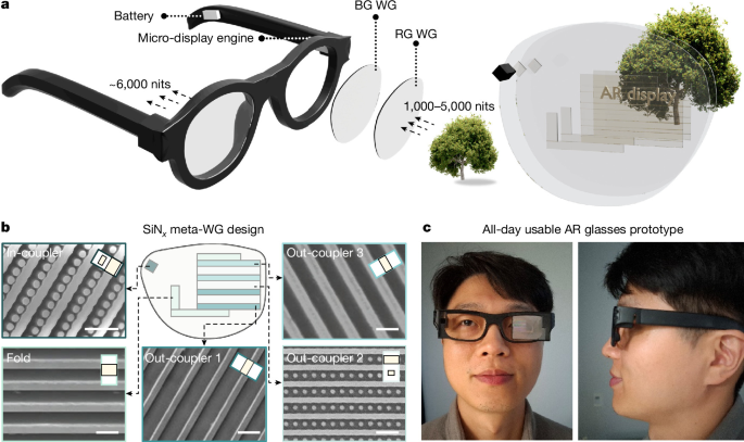
Researchers have developed a 1.5-millimetre-thick augmented reality lens using interwoven metasurfaces that delivers outdoor-visible brightness while solving the longstanding trade-off between field of view and eyebox size.
For more than a decade, the promise of true augmented reality eyewear has run headlong into fundamental optical physics. Designing a display that sits comfortably on a human face requires balancing three mutually hostile variables: field of view, eyebox volume, and optical efficiency. Expand the viewing angle, and the eyebox, the spatial window where the user's pupil can actually catch the image, shrinks to a pinhole. Enlarge the eyebox to accommodate natural eye movement and varying face shapes, and optical throughput plummets, demanding power-hungry microdisplays that generate uncomfortable heat and drain batteries within minutes.
Traditional diffractive optical waveguides, which rely on surface relief gratings etched into glass, have struggled to escape this trilemma. Because conventional gratings offer limited degrees of freedom in how they steer light, hardware developers have had to stack multiple thick glass plates or settle for dim, washed-out graphics that disappear under daylight. Now, a breakthrough in nanophotonics promises to bypass those compromises entirely through the use of spatially varying, interwoven metasurfaces.
The Nanoscale Architecture of Light Routing
Metasurfaces are flat, subwavelength optical elements composed of engineered nanoscale structures, often referred to as meta-atoms or nanopillars. Rather than relying on the gradual accumulation of phase shifts through curved, bulky glass lenses, metasurfaces introduce abrupt changes to the phase, amplitude, and polarization of light across an infinitesimally thin interface.
In conventional augmented reality waveguides, light from a microdisplay is injected into a transparent substrate via an input grating, travels through the glass using total internal reflection, and is gradually coupled out toward the eye by an exit grating. Most systems use simple periodic linear grooves. These grooves possess only a single grating vector, which severely restricts the pathways along which light can be guided and expanded.
The new architecture rethinks this approach by introducing an interwoven metasurface design. By spatially varying the geometry and orientation of nanostructures across the surface, the researchers synthesized several distinct grating vectors within a single shared physical layer. This interleaved configuration allows the optical element to control light propagation in multiple directions simultaneously. Instead of forcing light along a rigid, single-axis path that wastes photons, the metasurface distributes and expands the optical pupil across two dimensions with unprecedented precision.
Unlocking Unprecedented Optical Efficiency
The most striking achievement of this dual-layer metasurface waveguide is its raw luminance efficiency. In wearable displays, efficiency is measured in nits per lumen, indicating how much visible brightness reaches the eye for every unit of luminous flux produced by the projector engine. Typical commercial diffractive waveguides register efficiencies well below a few hundred nits per lumen. This forces designers to drive microLED or microOLED panels at peak power, triggering severe thermal constraints on delicate frames.
The interwoven metasurface prototype achieved an average luminance efficiency of 1,938 nits per lumen, with peak performance reaching 4,225 nits per lumen. This represents an order-of-magnitude leap over many existing optical combiners. By preserving the majority of the light injected by the optical engine, the system can produce sharp, saturated graphics without requiring heavy heat sinks or high-drain battery packs.
Crucially, these efficiency numbers were achieved without gutting other core specifications. The device delivers a 30-degree diagonal field of view paired with an 8 by 8 millimetre two-dimensional eyebox. An eyebox of this size is large enough to ensure that users do not experience sudden image clipping when shifting their gaze or adjusting the glasses on their nose, a common flaw in early consumer smart glasses.
Surviving the Glare of the Physical World
Laboratory demonstrations of augmented reality often hide a glaring flaw: they are calibrated for darkened testing rooms. The moment an engineer steps into the midday sun, ambient environmental illumination, which frequently exceeds 10,000 to 50,000 lux, completely overwhelms the virtual overlay. To stay readable outdoors, a display must pump out thousands of nits of perceived brightness directly to the retina.
Because the prototype preserves photon throughput so effectively, the researchers were able to demonstrate stable, clear virtual imagery under direct outdoor ambient illumination. The dual-layer metasurface waveguide cleanly decouples the projected digital layer from the real-world scene, preventing severe rainbow artifacts and stray ghost reflections that commonly plague multi-grating systems.
All of this optical control is contained within a form factor that is just 1.5 millimetres thick. At this scale, the entire optical combiner mimics the profile and weight of an ordinary corrective lens. By collapsing multidirectional beam steering into an ultra-thin dual-layer structure, the approach eliminates the cumbersome, multi-slab assemblies that have kept smart glasses looking like clinical laboratory hardware rather than daily apparel.
Moving from Nanofabrication to Mass Production
While the optical milestones are clear, bringing metasurface waveguides out of research facilities and into commercial manufacturing presents practical hurdles. Metasurfaces require sub-micrometre features with high aspect ratios, demanding manufacturing tolerances down to tens of nanometres across relatively large surface areas.
Historically, such nanostructures were patterned using electron-beam lithography, a precise but painfully slow process suited only for prototyping. To scale this technology for commercial distribution, manufacturers will need to leverage deep-ultraviolet lithography or advanced nanoimprint lithography (NIL). Nanoimprint techniques, which use a high-precision master stamp to replicate nanoscale patterns into optical resins on glass wafers, have matured rapidly, driven by investments across semiconductor foundries.
First documented in the journal Nature, the research provides a concrete blueprint for how nano-optics can resolve the systemic physical bottlenecks that have stalled augmented reality hardware. By proving that multiple grating vectors can co-exist across interwoven nanostructures, the study establishes a scalable design methodology for high-performance optical combiners.
Why It Matters
For industrial and field operations, the transition from bulky headsets to all-day wearable glasses is not a cosmetic luxury, it is an operational requirement. Frontline technicians servicing telecommunications towers, data centre facilities, and power grids require continuous visual guidance without looking away from high-voltage equipment or delicate fiber arrays. Current enterprise headsets are too heavy for eight-hour shifts and too dim to use on sunny outdoor cell towers.
A 1.5-millimetre waveguide delivering several thousand nits per lumen transforms what is feasible in the field. Technicians can wear standard-profile safety glasses capable of overlaying real-time schematics, AI-driven diagnostic telemetry, and remote-expert video feeds under any lighting condition. In data centre corridors where cooling fans create extreme acoustic noise, high-efficiency AR glasses provide silent, heads-up verification of port mappings and server rack configurations. By eliminating optical trade-offs at the physical level, metasurfaces bring ambient, hands-free computer vision into the regular working day.
More from Trends
RSS
Inside China's Coordinated Campaign to Build an AI-Native Generation
With mandatory curricula, entrance exam integration, and rural AI tutors, China is executing a massive state push to achieve universal AI literacy across 200 million students by 2030.
Securing Generative Biology: Inside the Defence-in-Depth Push for Biological AI
As AI models advance from generating protein structures to viable viral genomes, biosecurity researchers outline a multi-layered defence across data, models, and DNA synthesis.

Offshoring the Compute Boom: Washington Looks to Southeast Asia for Data Centers
Facing domestic grid bottlenecks and community backlash, US officials are promoting offshore AI infrastructure and chip manufacturing in the Philippines.